Bright Future Ahead for Thin Film Lithium Niobate
By: Milan Begliarbekov

Why Thin Film Lithium Niobate
Thin Film Lithium Niobate (TFLN) is rapidly becoming the new darling child of the telecommunications industry. Although lithium niobate itself is an old material with a proven 60-year history of utility as the active element in transducers and non-linear optical components, thin-film lithium niobate brings to the table even more exciting possibilities.
TFLN overcomes the biggest limitation of bulk lithium niobate: the inability to tightly confine light. While weak confinement was not an issue for sub-100G devices, this limitation, coupled with the relatively large bulk LN die sizes, led the industry to shift focus to other materials, such as Indium Phosphide. In the past decade, however, the newfound ability to mechanically exfoliate and etch TFLN (and its not-so-distant cousin lithium tantalate) has reinvigorated both academic and industrial research efforts in finding new applications for TFLN.

Putting TFLN to work
There is a growing consensus that thin-film lithium niobate will most likely become a key enabler of 1.6 and 3.2 terabit modules for data centers. While 200G devices will still use indium phosphide, the ultra-wide bandwidth, low insertion losses, and low switching voltages put TFLN in the running for the next generation of switches. Furthermore, the low Vπ-length product offers the added benefit of significantly reducing the overall device size, thereby enabling high-density heterogeneous integration and copackaging.
There is even better news on the horizon: in addition to the promise of sustaining the expansion of the telecom and hyperscale sectors, TFLN has the potential to disrupt computing as well. It has long been acknowledged that the physical phenomena that underpin the meteoric growth of AI hardware, namely Dennard Scaling and Amdahl’s Law are coming to an end. Denard scaling guarantees that the power density is roughly constant for a given die size while Amdahl’s law ensures that a speedup in latency can be brought about by increasing the number of processing cores. Recent studies showed that for smaller transistor sizes, the power requirements actually increase non-linearly with the transistor size. This seemingly disastrous limitation of conventional CMOS devices can only be overcome by a new paradigm of computing – a new architecture that looks beyond the confines of von Neumann machines and embraces new materials to carry out computation.
Analog and neuromorphic devices have long been slated as contenders to bring about this long-awaited change. Recently, several research groups experimentally demonstrated that TFLN-based modulators using time-division encoding are capable of achieving an impressive 60 Giga Operations per Second per Neuron in a photonic tensor core processor while consuming extremely little power. In essence, thin film lithium niobate holds tremendous promise not only for becoming the material of choice for high-speed communication but also as a key enabler of a new paradigm of computing. What will this paradigm look like? Only time will tell, but with hundreds of new researchers joining this field, exciting new ideas are bound to emerge.
Building a fab
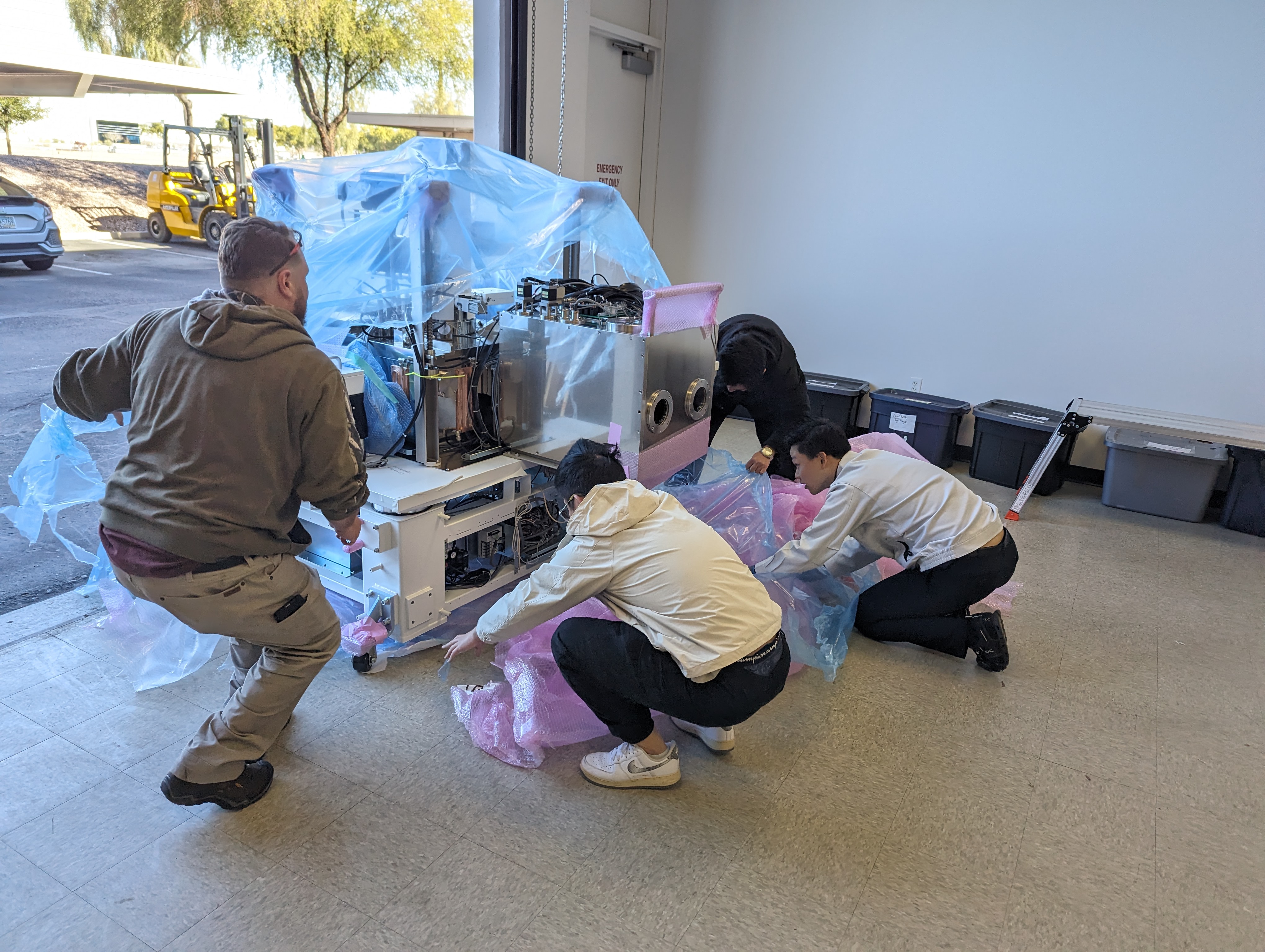
A major problem that is currently limiting mass adoption of thin film lithium niobate is the lack of a robust supply chain for TFLN wafers and the relative paucity of commercial fabs that will process TFLN. At QCi, we decided to dive head-first into this deep pool of possibilities and build a first of its kind fab devoted to TFLN processing. The fab, which will open to the public in Q1 of 2025 is located in Tempe, AZ, has both front-end and packaging capabilities for a 150 mm wafer line, as well as the ability to design, simulate, and characterize TFLN devices.